
The Critical Role of Silicon Interposers in Large-Size AI Chips
When people talk about the future of AI chips, the conversation usually starts with transistor nodes, model sizes, or memory bandwidth. But behind all of that sits a less glamorous, yet absolutely decisive, piece of technology: the silicon interposer. In large-size AI chips, the interposer is what makes heterogeneous integration practical at scale, tying together massive compute dies, multiple HBM stacks, and increasingly complex chiplet ecosystems into one high-performance package.
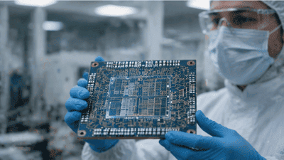
This is where advanced encapsulation stops being an afterthought and becomes part of the architecture itself. A silicon interposer is not just a passive bridge. It is the routing fabric, mechanical foundation, and often the bandwidth enabler for modern AI systems. Without it, many of today’s largest accelerators would be impossible to assemble economically, or at least impossible to build with the bandwidth and power efficiency they need. As AI chips grow larger and more modular, the interposer’s role only becomes more central.
Why Large AI Chips Need Interposers
Large AI chips are different from traditional processors in both scale and behavior. They are often designed to move staggering volumes of data between compute logic and memory, and they must do so within tight power and thermal limits. A monolithic die can only stretch so far before yield, reticle size, and routing congestion become serious problems. That is why designers increasingly split the system into multiple dies and place them on a silicon interposer.
The interposer solves several problems at once. It allows the logic die and HBM stacks to sit side by side at extremely fine pitch, enabling very wide interfaces that would be difficult to route on an organic substrate alone. It also provides a way to partition functionality across multiple dies, improving yield and design flexibility. In large AI packages, that matters a lot: the compute die can be optimized for logic density, while memory, I/O, and sometimes even cache or accelerator tiles are distributed across the package in a more economical way.
In short, the silicon interposer turns a collection of dies into a coherent system. That is exactly what heterogeneous integration is meant to achieve.
The Bandwidth Problem
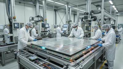
If there is one reason silicon interposers have become so important in AI, it is bandwidth. Training and inference workloads have become so data-hungry that the old model of moving signals through relatively narrow package traces is no longer enough. Compute units are starving for memory bandwidth, and the demand keeps rising as models get bigger and workloads become more parallel.
A silicon interposer helps by providing dense, short electrical pathways between dies. Instead of sending signals through long, lossy routes on a board, the interposer keeps everything local and highly parallel. This makes it possible to connect several HBM stacks around a large compute die and sustain the enormous throughput that modern AI accelerators require. The result is lower latency, lower energy per bit, and a more balanced system overall.
Without the interposer, many AI chips would be forced to compromise. They might use fewer memory stacks, narrower buses, or more aggressive signaling schemes that consume more power and deliver less bandwidth. In an era where every watt and every millimeter matter, those compromises can be fatal to competitiveness.
How Silicon Interposers Fit into Advanced Encapsulation
Advanced encapsulation is the broader discipline that makes this all work. A silicon interposer is only one part of the package stack, but it sits at a critical point where electrical, thermal, and mechanical requirements all converge. The interposer has to support microscopic routing, survive thermal cycling, align accurately with multiple dies, and integrate cleanly into the surrounding package substrate.
In practice, that means the interposer becomes a design object in its own right. Its thickness, via structure, routing layers, and die placement pattern all affect the package’s final behavior. Engineers must decide whether to use a passive silicon interposer, a bridge-like approach, or a more integrated 2.5D/3D configuration. These decisions are not trivial because they influence cost, yield, and long-term reliability.
The package no longer exists to merely protect the chip. It defines the chip’s actual performance envelope. That is why advanced encapsulation and silicon interposers are inseparable in the large AI chip discussion.
Interposers and Heterogeneous Integration
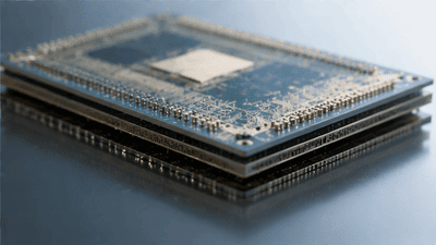
Heterogeneous integration is all about mixing different dies, technologies, and sometimes even process nodes within one system. Silicon interposers are ideal for this because they provide a neutral, high-density platform for interconnect. They can host logic dies from a leading-edge node, HBM from a memory specialist, and possibly I/O or control chiplets from another process node or supplier.
This flexibility matters. It allows chip designers to optimize each function independently instead of forcing everything onto the same die. That can improve yield, reduce cost, and make product roadmaps more modular. In the AI world, where product cycles are short and demand is volatile, modularity is a major advantage. A company can reuse an interposer-based platform across multiple accelerator generations, swapping compute chiplets or memory configurations while preserving much of the package architecture.
The interposer also supports more complex systems over time. As chiplets proliferate, the package may include more than just compute and memory. It may contain specialized accelerators, cache dies, security blocks, or interface chips. The interposer offers a common routing fabric that ties them all together without requiring a radical redesign of the entire substrate or board.
Design Trade-Offs: Performance vs. Cost
The advantages of silicon interposers are clear, but they come with a price. Interposers add cost, complexity, and manufacturing risk. That is why the industry still treats them as a premium solution, especially for high-end AI chips where the bandwidth benefits justify the expense.
One of the biggest trade-offs is manufacturing yield. A large interposer must be fabricated with very fine features and very low defectivity. If the interposer is too large or too complex, yield falls, and the cost per usable package rises quickly. Add multiple large dies and several HBM stacks, and the entire stack becomes sensitive to any defect in any layer. This makes process control essential.
Another trade-off is thermal behavior. Silicon is good at distributing heat laterally compared with many organic materials, but a large AI package still creates hotspots, especially where compute density is highest. The interposer itself may help spread heat, but it can also complicate thermal flow depending on the package architecture. Designers must balance electrical routing needs against the realities of heat extraction.
Cost and performance are therefore locked in a constant negotiation. That is normal in advanced packaging, but silicon interposers make the negotiation much sharper because they sit at the center of the most expensive AI systems in the market.
Why Large Size Matters So Much
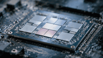
The phrase “large size AI chips” deserves special attention because size changes everything. As dies get larger, the chances of defects rise, the complexity of routing increases, and the mechanical stress on the package grows. Large dies also run into practical limits on reticle size and fabrication economics, which is why splitting them across multiple chiplets and interposer-based packages is so appealing.
For very large AI accelerators, the package may be physically large enough to challenge warpage control, alignment accuracy, and substrate reliability. The interposer helps by providing a rigid, precise foundation that can host multiple dies with tight spacing and known geometry. In other words, it is not just about communication bandwidth. It is also about package stability at scale.
Large packages also tend to have more extreme power delivery requirements. The interposer can help distribute power more effectively, but it must be designed carefully so that power and signal paths do not interfere with one another. That is one reason interposer layout is such a multidisciplinary problem. It sits at the intersection of electrical design, materials engineering, thermals, and mechanical reliability.
Alternative Paths and Why They Matter
Silicon interposers are critical, but they are not the only solution in the heterogeneous integration toolbox. Fan-out packaging, organic substrates with very fine routing, and emerging 3D bonding technologies all compete with or complement interposer-based architectures. Each approach has a different balance of cost, density, performance, and manufacturability.
Fan-out, for example, may offer a lower-cost path for some mobile or mid-range AI applications, though it generally cannot match the routing density of a silicon interposer for the largest accelerator packages. Organic substrates are cost-effective and widely used, but they often require an interposer when bandwidth and pitch become too aggressive. 3D integration with hybrid bonding may eventually reduce dependence on large interposers for some use cases, but that technology introduces its own thermal and design challenges.
So the role of the silicon interposer is not to eliminate all other packaging approaches. It is to occupy the sweet spot where performance is high enough to justify its cost and where alternative technologies still fall short. For large-size AI chips, that sweet spot is very much real today.
Supply Chain and Capacity Pressure
Another reason silicon interposers are so important is that they sit in a constrained part of the supply chain. The manufacturing of interposers requires precise process capability, specialized equipment, and careful coordination with the rest of the packaging flow. In an AI boom, that makes interposers a strategic bottleneck.
When demand for accelerators surges, it is not enough to have wafers ready. You also need interposer capacity, substrate availability, HBM supply, and advanced assembly lines that can put everything together. Any shortage in that chain can delay shipments and push customers toward alternative architectures or vendors. This is one reason foundries and packaging houses have invested heavily in advanced packaging capacity over the past few years.
The interposer has become a supply chain signal. If it is hard to get, you know the AI package market is tight. If it is abundant, the market is relaxing. At the moment, for top-end AI systems, it is still closer to the former.
The Future: Smaller, Smarter, and More Integrated
Looking ahead, the role of silicon interposers may evolve rather than disappear. Future AI packages could use smaller, more specialized interposers, hybrid schemes that combine interposer and 3D bonding, or even new materials that preserve the routing advantages while lowering cost and improving thermal behavior. The package landscape is still in motion.
What is unlikely to change is the need for some kind of dense integration fabric. Whether that fabric is a silicon interposer, a bridge, or a bonded 3D structure, the problem remains the same: large AI chips need enormous bandwidth, careful thermal management, and a way to combine many different dies into one cohesive system. Silicon interposers are currently the most mature answer to that problem.
As AI systems grow more modular and more power-hungry, the interposer may become even more central. It could support not only memory and compute but also optical links, power delivery innovations, or more complex chiplet topologies. In that future, the interposer is less a passive middle layer and more a platform for system integration.
Conclusion
Silicon interposers are critical because they make large-size AI chips possible in a practical, high-performance, and manufacturable way. They solve the bandwidth problem, enable heterogeneous integration, support modular design, and provide a stable platform for the most demanding advanced packaging architectures. Without them, many of today’s flagship AI accelerators would either be too slow, too power-hungry, too large, or too costly to build at scale.
That is why advanced encapsulation and silicon interposers belong in the same conversation. They are part of the same system-level answer to the limits of monolithic scaling. As AI chips continue to grow in size and ambition, the interposer will remain one of the most important pieces of silicon in the package—quiet, invisible to most users, but absolutely essential to the performance they expect.
You May Like

Narrowing Spread Between NAND Spot and Contract Prices in 2026 – A Signal
By 2026, one of the most watched metrics in the NAND flash market has started to shift in a subtle but meaningful way: the spread between spot prices and long‑term contract prices is narrowing. For casual observers, this may look like just another incremental change in a notoriously volatile industry. For memory makers, module houses, device OEMs, and data center buyers, however, a tightening gap between spot and contract prices is a signal—a reflection of evolving supply–demand balance, risk perceptions, and strategic behavior on both sides of the market.

Price Divergence Trading Strategies Between NAND Flash and DRAM ETFs
NAND flash and DRAM sit at the core of AI storage and computing power. Both are memory, but they are not the same business. DRAM is main memory—fast, volatile, and central to high‑bandwidth workloads like AI training and inference. NAND is non‑volatile storage—slower than DRAM, but crucial to persistent data and large‑scale object storage. The cycles that drive their pricing and margins overlap, yet they often diverge. That divergence is where trading strategies between NAND and DRAM ETFs become interesting.
China’s HBM Localization Progress: The Catch-Up Pace of CXMT and XMC
China’s drive to localize advanced memory technologies has accelerated over the past several years. High-Bandwidth Memory (HBM) sits near the center of that strategy because it is integral to AI accelerators, high-performance computing (HPC) and other strategic compute platforms. Two domestic players—ChangXin Memory Technologies (CXMT) and XMC (Xianghui Memory, commonly referred to as XMC)—have become focal points in assessing how quickly China can close the gap with international incumbents on HBM die, stacking, and packaging.
Thermal Simulation Challenges and Solutions in 3DIC AI Chip Design
As AI workloads push chips to deliver ever higher compute density, designers are increasingly turning to three‑dimensional integration (3DIC) to stack dies vertically and pack more functionality into limited footprints. While 3DIC architectures unlock significant performance and bandwidth advantages, they also introduce complex thermal behaviors that are far harder to predict and manage than in traditional 2D layouts.

An Attempt at Compiling a Memory+Compute Fusion Thematic Index – A Dual-Track Framework
Most AI investors talk about “compute” as if it were the whole story: GPUs, accelerators, chips, cores. But every one of those cores needs somewhere to read from and write to. Memory and storage define how wide the data highway really is. In practice, AI performance is a fusion of compute and memory, not a solo act. So why do so many indices and ETFs separate them into different silos—one for semiconductors, one for memory, one for data centers—when the actual workloads keep blending them?
Surging Demand for Laser Drilling and Plasma Dicing Equipment in Advanced Packaging
Advanced packaging has become one of the semiconductor industry’s most important growth engines, and it is now pulling a surprising set of process tools into the spotlight. Among the most in-demand are laser drilling and plasma dicing equipment. These machines sit close to the heart of heterogeneous integration, fan-out packaging, wafer thinning, TSV formation, glass substrate processing, and other advanced flows where precision, yield, and throughput matter enormously. As packaging moves from a back-end afterthought to a strategic platform, the equipment used to shape, open, and separate materials has become just as important as the dies themselves.

D2D Interface Bandwidth and Latency Comparison in Chiplet Architectures
Chiplet architecture has turned the package into a real performance battleground. Once multiple dies are placed side by side or stacked within the same advanced package, the quality of the die-to-die, or D2D, interface becomes one of the most important determinants of system behavior. Bandwidth is no longer a nice-to-have metric, and latency is no longer a small implementation detail. Together, they shape whether a chiplet system feels nearly monolithic or frustratingly fragmented.

Stock Selection Logic and Alpha Validation of ESG-Themed Semi ETFs
Semiconductor themed ETFs are no longer just about growth and cycles. A growing subset now layers environmental, social, and governance (ESG) criteria on top of traditional sector exposure. These ESG semi ETFs promise two things at once: access to one of the market’s most powerful secular themes, and alignment with sustainability and governance standards. The pitch is appealing, but it raises two hard questions. First, how exactly are these stocks being selected? Second, does the ESG overlay help, hurt, or leave alpha unchanged?